Nvidia Graphics Card
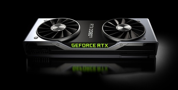
The main thing that distinguished the older models of the 30th series also applies to the younger ones: the performance increases, and the FPS price decreases. The GeForce RTX 3060 should cost even less than the RTX 2060. Plus, ironically, the RTX 3060 now has the most VRAM in the entire lineup, except for the RTX 3090. Tested using the Palit Dual OC as an example
At the moment, NVIDIA has fully equipped the top of the GeForce lineup with 30 devices based on Ampere architecture chips. Compared to their predecessors, all new NVIDIA offers have significantly improved not only in absolute performance metrics, but also in performance per unit of recommended cost. Nevertheless, even the GeForce RTX 3060 Ti at an official price of $ 399 (or 39,990 Russian rubles) is not available to all gamers or simply has redundant capabilities for those who play only sporadically and do not use demanding working applications. The lion’s share of sales from graphic card manufacturers are devices priced below $ 400 – this market segment was the next zone of expansion for the Ampere architecture. The GeForce RTX 3060 is the first of its kind in a new generation of NVIDIA accelerators and, at the same time, the cheapest graphics card ever released under the RTX brand.
In the meantime, AMD is hesitating to release models of similar performance on second-generation Navi chips, buyers who intend to change their GeForce GTX 1060 and Radeon RX 570/580 to something more powerful and at the same time save money have no choice but to GeForce RTX 3060. The main thing is that the unprecedented shortage of computer components bypasses the novelty. NVIDIA will get more compact GPUs that power the RTX 3060 from each silicon wafer. In addition, the chipmaker announced that cryptominers have absolutely nothing to catch in this case: the RTX 3060 hashrate will be artificially limited at the level of agreement between the BIOS and the driver. Whether these measures helped to saturate the demand for a video card (and in this price category it is especially large), we can find out in the first days after the publication of the review – sales of the RTX 3060 will start today. In the meantime, let’s find out what exactly the new product will be able to offer gamers (and thrifty professionals) at its cost.
NVIDIA traditionally builds a lineup of high-performance graphics accelerators around GPUs of three categories, numbered 102, 104 and 106 with the corresponding generation prefix. On the basis of GA102 and GA104, four devices of the GeForce 30 series have already appeared, and now the GA106 processor should take over the baton. In terms of rendering functions and configuration, the main building block of NVIDIA architecture – the streaming multiprocessor (SM) – the junior GPU is no different from the flagship chips. Readers can brush up on what Ampere is and how it compares to its predecessor Turing logic in our in-depth review. And in order to get silicon corresponding to the price category of the GeForce RTX 3060, NVIDIA only changed the quantitative indicators. So, GA106 has 30 SM, while fully functional GA104 and GA102 crystals have 48 and 84 units, respectively.
The direct analogue of GA106 in the Turing family is, of course, the TU106 chip, which underlies the GeForce RTX 2060, RTX 2060 SUPER and RTX 2070, but if GA104 and GA102 are at least not inferior to their ancestors in terms of the number of SM, then GA106 is a step in the opposite direction. : The TU106 has a total of 36 SMs, while the GA106 has only 30. As a result, the L2 cache size could be safely reduced from 4 to 3 MB. But the relatively small number of SMs more than compensates for the doubled volume of real ALUs of standard precision inside each of them. This is a characteristic feature of Ampere, which still does not guarantee double performance in all situations, except for isolated synthetic benchmarks, but there are applications that fit well with such an architecture (including games with ray tracing), not to mention a lot of other optimizations inherent in Ampere. At first glance, the number of rasterization units in the GA106 is also small – only 48 versus 64 in the TU106, but this cannot be considered a compromise solution on the part of NVIDIA. It’s just that the ROP array is now independent of the RAM controllers and provides just such a pixel fill rate that corresponds to the throughput of the rasterizers – no more and no less (the TU106 had ROPs in abundance). https://jiji.com.gh/adenta-municipal/computer-hardware/nvidia-graphics-card-k7R0mGD8YIFUphM7nloJxfpY.html
Streaming Multiprocessor (SM) Configuration
32/64 of 96 (shared with shared memory)
Up to 64 of 128 (shared with shared memory)
GPU Programmable Computing Units
Fixed Function GPU Blocks
Be that as it may, the dramatically increased number of shader ALUs in the GA106 crystal affected the processor’s component budget: it is 12 billion transistors, which is 1.1 billion more than the TU106 data. But thanks to the high density of the Samsung 8 nm process technology, the GA106 crystal turned out to be very compact: its area is only 276 mm2.
a large increase in energy efficiency, and in relatively small GPUs, the power scales less well together with the number of main computational units.